
Semiconductor and IC Packaging | ATMA
Semiconductor and IC Packaging1. SemiconductorA semiconductor is a material whose electrical conductivity lies between that of a conductor and an insulator, most commonly silicon (Si). By controlling its electrical properties through fabrication processes, semiconductors can be used to manufacture transistors and integrated circuits, which form the fundamental basis of modern electronics. They are extensively applied in computers, telecommunications, AI (Artificial Intelligence), automotive electronics, and various smart devices.2. PackagingPackaging is the process of connecting a fabricated semiconductor (Die) to external circuitry and providing protection. It enables electrical interconnection, mechanical protection, and heat dissipation, allowing the chip to operate reliably in a wide range of electronic products. Common packaging types include BGA, QFN, and CSP, with advancements extending to advanced packaging technologies such as SiP, Fan-Out, and 3D packaging.★★★ Screen Printing Applications 1. Solder Paste Printing Solder paste is printed onto the surface of substrates or package carriers for subsequent chip or component soldering, requiring high precision and uniform thickness control.2. Conductive Silver Paste Printing Conductive silver paste is printed to form electrical circuits or contact points, commonly used in chip interconnection, sensors, and power modules.3. Insulating Material Printing Insulating materials are printed onto substrate surfaces to form insulation or protective layers, preventing short circuits and enhancing electrical reliability.4. Encapsulation Material Printing Encapsulation adhesive is printed or dispensed between the chip and the substrate to enhance structural strength and thermal cycling resistance.5. Microvia Filling Printing High-viscosity materials are used to fill microvias or through-holes, commonly applied in IC substrates and advanced packaging processes.6. Solder Mask Printing A solder mask layer is printed on the circuit surface to protect the traces and prevent solder bridging. These screen-printing processes typically require micron-level alignment accuracy, high uniformity, and long-term process stability, making them critical technologies in semiconductor packaging and IC substrate manufacturing.★★★ Process Requirements Micron-level alignment accuracy, ultra-low contamination processes, stable printing pressure control, and high repeatability in positioning.★★★ Key Requirements High-resolution printing, uniform material deposition, low defect rates, and long-term process stability to ensure packaging yield and product reliability.★★★★Mass Production Process Challenges1. Difficulty in Fine-Line Printing ▲Customer Challenges In advanced packaging and IC substrate line refinement, traditional printing processes often encounter issues such as line width non-uniformity, edge roughness, or short-circuit defects. ▲Proposed Solution High-precision CCD visual registration, precision sliding table positioning mechanisms, and high-tension screen control enhance registration accuracy and printing stability. ▲Tangible Benefits Improves fine-pattern printing capability, reduces short-circuit and defect rates, and stabilizes yield in advanced manufacturing processes.2.Unstable yield in micro-via plugging ▲Customer Challenges In IC substrates or advanced packaging, micro-via filling is often incomplete, leading to voids or resin overflow. ▲Proposed Solution High-stability printing pressure control, precise squeegee angle adjustment, and optimized material flow management design. ▲Tangible Benefits Enhances via-filling completeness, reduces void defects, and improves packaging reliability.3.Instability in Long-Term Mass Production ▲Customer Challenges Extended production may lead to reduced printing thickness and diminished pattern consistency, ultimately compromising product quality. ▲Proposed Solution High-rigidity machine structure, precision linear guide-ways, and servo control systems ensure stable operation. ▲Tangible Benefits Ensures consistent product quality during long-term mass production by minimizing process fluctuations.4.Long Setup Time for Multi-Product Changeovers ▲Customer Challenges Diverse packaging products require frequent line changes, resulting in increased downtime. ▲Proposed Solution Digitalized recipe management and rapid changeover positioning mechanism. ▲Tangible Benefits Shortens machine setup time to increase equipment utilization and boost production efficiency.5.High-precision processes are extremely sensitive to contamination. ▲Customer Challenges Micron-level packaging processes are prone to defects caused by dust or ink contamination. ▲Proposed Solution Clean design, electrostatic elimination, and enclosed printing structure. ▲Tangible Benefits Reduces contamination risks and enhances yield for advanced packaging products. Browse ATMA screen printing equipment by category to reach the right machine type faster. Use categories to narrow by format—sheet, cylinder press or roll-to-roll—and then compare models and accessories.
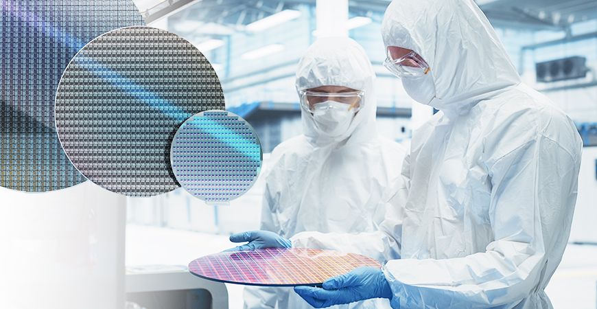
Semiconductor and IC Packaging
Process Technology,Wafer Related,IC Classification,Semiconductor Materials.Advanced Packaging,Packaging Process,Testing and Reliability
Semiconductor and IC Packaging
1. Semiconductor
A semiconductor is a material whose electrical conductivity lies between that of a conductor and an insulator, most commonly silicon (Si). By controlling its electrical properties through fabrication processes, semiconductors can be used to manufacture transistors and integrated circuits, which form the fundamental basis of modern electronics. They are extensively applied in computers, telecommunications, AI (Artificial Intelligence), automotive electronics, and various smart devices.
2. Packaging
Packaging is the process of connecting a fabricated semiconductor (Die) to external circuitry and providing protection. It enables electrical interconnection, mechanical protection, and heat dissipation, allowing the chip to operate reliably in a wide range of electronic products. Common packaging types include BGA, QFN, and CSP, with advancements extending to advanced packaging technologies such as SiP, Fan-Out, and 3D packaging.
★★★ Screen Printing Applications
1. Solder Paste Printing
Solder paste is printed onto the surface of substrates or package carriers for subsequent chip or component soldering, requiring high precision and uniform thickness control.
2. Conductive Silver Paste Printing
Conductive silver paste is printed to form electrical circuits or contact points, commonly used in chip interconnection, sensors, and power modules.
3. Insulating Material Printing
Insulating materials are printed onto substrate surfaces to form insulation or protective layers, preventing short circuits and enhancing electrical reliability.
4. Encapsulation Material Printing
Encapsulation adhesive is printed or dispensed between the chip and the substrate to enhance structural strength and thermal cycling resistance.
5. Microvia Filling Printing
High-viscosity materials are used to fill microvias or through-holes, commonly applied in IC substrates and advanced packaging processes.
6. Solder Mask Printing
A solder mask layer is printed on the circuit surface to protect the traces and prevent solder bridging. These screen-printing processes typically require micron-level alignment accuracy, high uniformity, and long-term process stability, making them critical technologies in semiconductor packaging and IC substrate manufacturing.
★★★ Process Requirements
Micron-level alignment accuracy, ultra-low contamination processes, stable printing pressure control, and high repeatability in positioning.
★★★ Key Requirements
High-resolution printing, uniform material deposition, low defect rates, and long-term process stability to ensure packaging yield and product reliability.
★★★★Mass Production Process Challenges
1. Difficulty in Fine-Line Printing
▲Customer Challenges
In advanced packaging and IC substrate line refinement, traditional printing processes often encounter issues such as line width non-uniformity, edge roughness, or short-circuit defects.
▲Proposed Solution
High-precision CCD visual registration, precision sliding table positioning mechanisms, and high-tension screen control enhance registration accuracy and printing stability.
▲Tangible Benefits
Improves fine-pattern printing capability, reduces short-circuit and defect rates, and stabilizes yield in advanced manufacturing processes.
2.Unstable yield in micro-via plugging
▲Customer Challenges
In IC substrates or advanced packaging, micro-via filling is often incomplete, leading to voids or resin overflow.
▲Proposed Solution
High-stability printing pressure control, precise squeegee angle adjustment, and optimized material flow management design.
▲Tangible Benefits
Enhances via-filling completeness, reduces void defects, and improves packaging reliability.
3.Instability in Long-Term Mass Production
▲Customer Challenges
Extended production may lead to reduced printing thickness and diminished pattern consistency, ultimately compromising product quality.
▲Proposed Solution
High-rigidity machine structure, precision linear guide-ways, and servo control systems ensure stable operation.
▲Tangible Benefits
Ensures consistent product quality during long-term mass production by minimizing process fluctuations.
4.Long Setup Time for Multi-Product Changeovers
▲Customer Challenges
Diverse packaging products require frequent line changes, resulting in increased downtime.
▲Proposed Solution
Digitalized recipe management and rapid changeover positioning mechanism.
▲Tangible Benefits
Shortens machine setup time to increase equipment utilization and boost production efficiency.
5.High-precision processes are extremely sensitive to contamination.
▲Customer Challenges
Micron-level packaging processes are prone to defects caused by dust or ink contamination.
▲Proposed Solution
Clean design, electrostatic elimination, and enclosed printing structure.
▲Tangible Benefits
Reduces contamination risks and enhances yield for advanced packaging products.
Customer Favorites
 Download
 Semiconductor and IC Packaging | ATMA
Browse our screen printer catalog to compare models by printing format, automation level, and line compatibility—then narrow to the best-fit options.
Since 1979, ATMA has focused on screen printing equipment, supporting buyers in selecting a screen printer and matching accessories like feeders and air dryers.
Tell us your material and output goals—ATMA will propose a screen printer setup and a clear shortlist to move forward.


